High Bandwidth Memory (HBM)
High Bandwidth Memory (HBM) signifies a high-speed computer memory interface, customarily utilized in graphics cards, for the effective management of vast amounts of data and high-resolution videos. HBM, a type of stacked memory, was developed by AMD and Hynix to overcome the limitations of traditional memory architecture and to meet the demands of increasingly sophisticated technology. HBM design utilizes stacked memory chips and an intricate grid of microscopic channels to deliver a high level of data transfer. This technology provides higher bandwidth, power efficiency, and compactness compared to older DRAM technologies such as GDDR5 and DDR4.
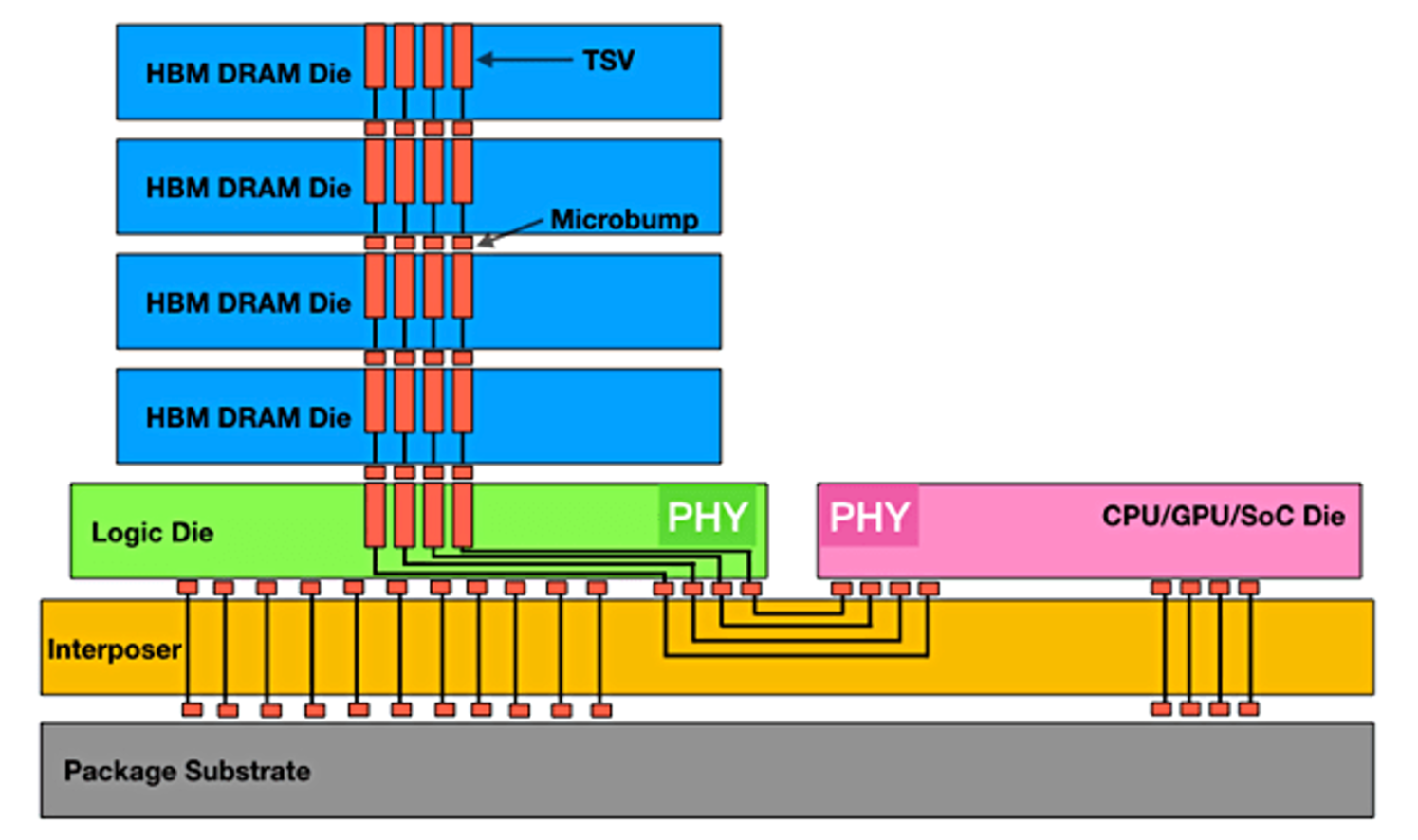
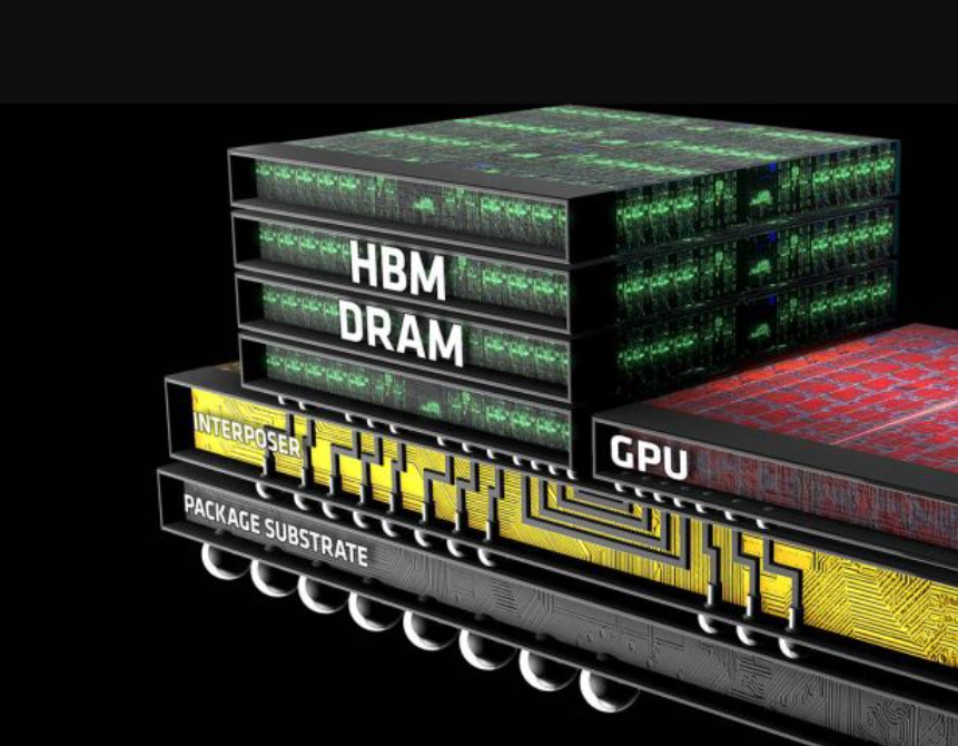
HBM technology’s primary distinction lies in its vertical stacking of DRAM dies, interconnected using Through-Silicon Vias (TSVs). These TSVs create a shorter data path, resulting in faster, more efficient data transfer and lower power consumption. The memory stacks are placed directly on the GPU die, which further shortens the electrical path, reducing latency and enhancing the overall performance.
The first generation of HBM, HBM1, was introduced in 2015, offering a significant leap in bandwidth compared to its predecessor, GDDR5. This leap was achieved by widening the memory bus to 1024-bit, a stark contrast to the 32-bit and 64-bit buses found on traditional DRAM. HBM1 could deliver a bandwidth of 128GB/s per stack, a substantial improvement over the 28GB/s offered by GDDR5. However, HBM1 had a limitation of only 4GB per stack, which was addressed in the subsequent generation, HBM2.
HBM2, released in 2016, doubled the bandwidth of HBM1 to an impressive 256GB/s per stack and increased the total capacity per stack to 8GB. This enhancement enabled more extensive data processing and more complex simulations, catering to the requirements of high-end graphics cards, supercomputers, and data centers.
In 2018, HBM2E was introduced, further pushing the capacity per stack to 16GB and a bandwidth of 410GB/s per stack. HBM2E is particularly useful in AI and machine learning applications, which require high-speed, high-capacity memory.
The future of HBM technology holds exciting potential. HBM3, the next generation of this technology, promises to deliver even higher bandwidth and capacity. It is expected to offer twice the speed of HBM2E, and with a potential capacity of 64GB per stack, it will be ideally suited for applications demanding substantial memory resources, such as virtual reality, AI, and machine learning.
In conclusion, HBM represents a significant technological advancement and a paradigm shift in memory architecture. It offers a solution to the growing demand for high-performance, power-efficient memory in a wide array of applications. Its unique vertical stacking design and use of TSVs have redefined the standards for memory speed and capacity. With each new iteration, HBM continues to push the limits of memory technology, ushering in a new era of computing power and capabilities.

Advanced Memory Technology
Advanced memory technology is a burgeoning field that continually pushes the boundaries of data storage capabilities. It encompasses a broad spectrum of innovations, from the evolution of traditional RAM and flash memory to the exploration of next-generation storage mediums such as phase-change memory, resistive RAM, and magnetic RAM. These cutting-edge technologies offer potential improvements in data retention, speed, capacity, and power efficiency.
Innovation in this field is driven by the unceasing demand for more efficient and faster data storage solutions. As we increasingly rely on digital tools and devices in various aspects of our lives, from personal use to business operations, the need for advanced memory technology becomes more pronounced. For instance, complex tasks such as AI processing, 3D rendering, and big data analysis require advanced memory technology to ensure seamless execution.
One exciting development in this field is the creation of non-volatile memory. Unlike traditional memory systems that lose data when power is lost, non-volatile memory retains information even when the device is turned off. This technology can significantly improve reliability and energy efficiency in a wide range of devices, from smartphones to supercomputers.
Another promising aspect of advanced memory technology is the development of quantum memory. This futuristic technology can store vast amounts of data in a minuscule physical space, leveraging the principles of quantum physics. Though still in its nascent stages, quantum memory holds the potential to revolutionize storage systems, leading to unprecedented computational power and efficiency.
In conclusion, advanced memory technology is a dynamic and rapidly evolving field that promises to redefine our data storage capabilities. While there are still many challenges to overcome, the progress made thus far gives us a glimpse into a future where data storage is faster, more efficient, and more reliable than ever before.
Interface Architecture and Specifications
Interface architecture and specifications are crucial components in the realm of information technology and software development. The interface architecture refers to the orderly arrangement and design of software interfaces. It primarily focuses on the interaction between multiple software components and how they communicate and interrelate with each other. On the other hand, interface specifications define the rules and standards that govern this interaction and communication within the system.
The architecture provides a blueprint or a map that illustrates how different software elements interact and integrate to form a complete system. It outlines the functionality, behavior, and structure of software interfaces. The specifications, meanwhile, detail the technical aspects of these interfaces, such as methods, protocols, and data formats to be used.
Both the architecture and specifications play a pivotal role in ensuring the system’s efficient operation. They provide software developers with a clear and concise overview of how the system should function. This aids in debugging, modifying, or enhancing the software as it provides them with a structure to follow and standards to adhere to.
Moreover, these two aspects also contribute to the system’s flexibility and scalability. Since they offer a comprehensive view of the system’s operation, they make it easier for developers to add new features or components to the system. Additionally, they ensure that these additions will not disrupt the overall operation of the system, making the system more adaptable to changes and advancements.
In conclusion, interface architecture and specifications serve as the backbone of any software system. They provide the structure and rules needed for the system to function optimally, and they also pave the way for the system’s future growth and development.

HBM2 – Second Generation High Bandwidth Memory
The second generation High Bandwidth Memory, commonly referred to as HBM2, is an advanced form of memory technology that has significantly impacted the computing industry. It is a high-performance RAM interface designed by AMD, and later adopted by JEDEC as an industry standard. This technology emerged as an answer to the increasing need for more efficient and effective memory solutions in high-performance computing applications, such as graphics processing units (GPUs), server farms, and data centers.
HBM2 improves upon its predecessor, HBM1, by offering double the bandwidth per pin, which essentially means it can transmit more data simultaneously. This improvement in bandwidth translates to superior performance in applications that demand high-speed data transmission. HBM2 memory technology has a 1024-bit wide interface, which is considerably wider than traditional memory technologies. This allows it to deliver a higher level of performance while using less power.
One of the distinguishing features of HBM2 is its stacked architecture. Unlike traditional memory chips that are laid out flat, HBM2 chips are stacked vertically. This design allows for a more compact footprint, which is especially important in applications where space is at a premium.
The use of HBM2 has significant implications for the future of computing. The ability to deliver greater performance in a smaller form factor opens up new possibilities for the design of GPUs and other high-performance computing applications. Furthermore, the lower power consumption of HBM2 is a critical factor in the drive towards more energy-efficient technology. In the face of ever-increasing data volumes and the need for faster processing speeds, HBM2 stands out as a revolutionary innovation in memory technology. Its adoption and further development will likely continue to shape the future of the computing industry.
HBM2E – Enhanced HBM2 with Improved Performance
HBM2E is the next-generation of High-Bandwidth Memory (HBM2), an advanced solution primarily used in high-performance computing, advanced graphics, and network systems. The inception of HBM2E represents a significant advancement in memory technology, offering considerable improvements in performance, capacity, and power efficiency over its predecessor.
HBM2E can deliver up to 3.2 gigabits per second (Gbps) of memory speed per pin, which represents a 33% increase over the top speed of 2.4 Gbps offered by HBM2. Additionally, HBM2E can support a higher capacity per stack, reaching up to 24GB as compared to the 8GB limit of HBM2. These enhancements, combined with the inherent advantages of HBM design—such as a wide I/O interface, 3D stacking, and reduced power consumption—make HBM2E an exceptional choice for demanding applications that require massive data processing capabilities. HBM2E’s superior performance is poised to drive forward technological innovation in areas such as artificial intelligence, machine learning, and high-performance computing. As such, HBM2E is not merely an evolution of HBM2; it is a cutting-edge memory solution that delivers unprecedented speed, capacity, and efficiency, paving the way for the next generation of advanced computing systems.

HBM3 – Third Generation High Bandwidth Memory
HBM3, or the third generation of High Bandwidth Memory, is a cutting-edge technology that is designed to significantly improve performance in high-end computing systems. Developed as an upgrade over its predecessor, HBM2, HBM3 offers enhanced data transfer rates, superior power efficiency, and increased memory capacity. This advancement in technology is aimed at accommodating the ever-growing demands of data-intensive applications, including artificial intelligence, machine learning, and high-performance computing.
HBM3 utilizes a vertically stacked DRAM die configuration, referred to as 3D stacking, in which several layers of memory cells are stacked on top of each other. This architecture results in a compact, high-density memory solution that can provide much higher bandwidth than traditional DRAM technologies. Moreover, HBM3 incorporates advanced features such as error correction, which contributes to improved reliability and robustness of the system.
An important aspect of HBM3 technology is its use of through-silicon vias (TSVs) and microbumps for interconnecting the stacked memory cells. This innovative approach ensures high-speed data transfer and reduced power consumption. It also allows HBM3 to deliver a far greater bandwidth per watt than other memory technologies, thereby enabling more efficient and powerful computing systems.
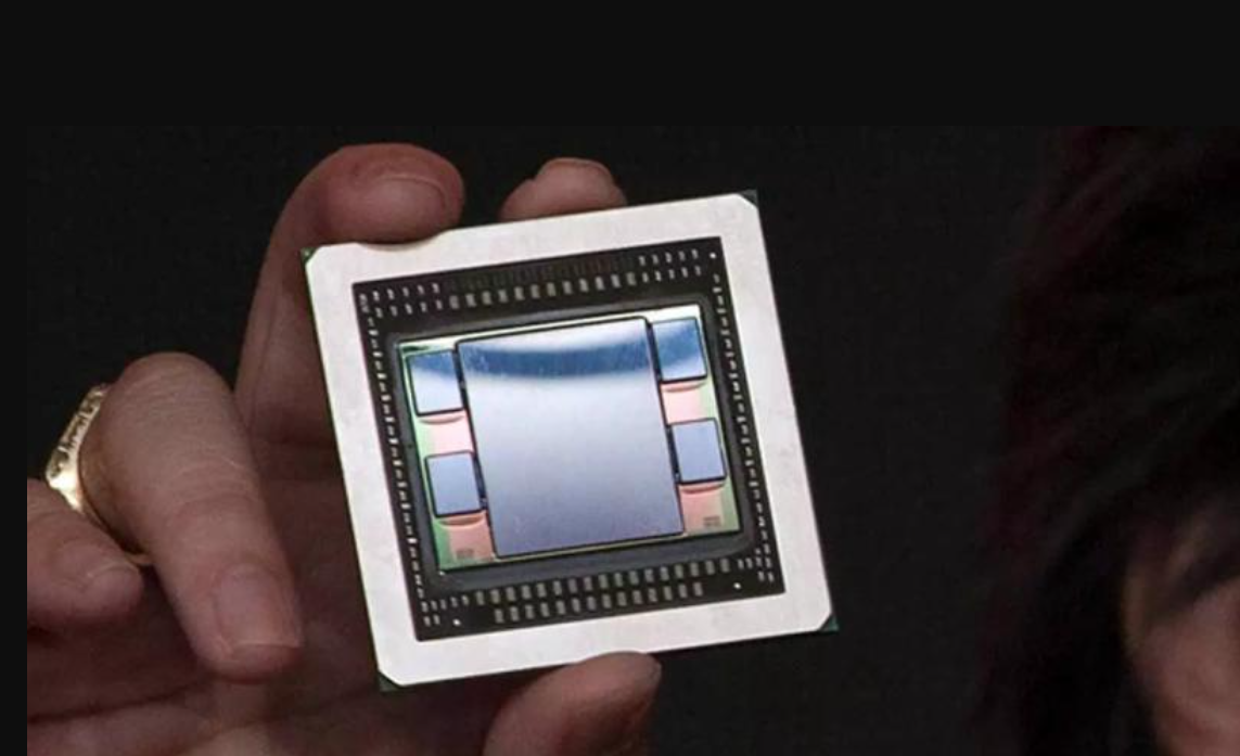
An emerging trend is the integration of HBM3 memory directly onto a processor or graphics chip, creating a ‘package-on-package’ configuration. This design further enhances the performance by reducing the distance data has to travel, thus improving data transfer speed and reducing latency.
In conclusion, HBM3 represents a significant leap forward in memory technology. Its high bandwidth, increased capacity, and power efficiency make it an ideal solution for next-generation computing systems. Despite being relatively new, HBM3 has the potential to revolutionize high-performance computing, and it is expected to play a crucial role in the future of technology.
HBM3E – Extended HBM3 Capabilities
HBM3E, also known as High Bandwidth Memory 3 Extended, is a significant advancement in memory technology that offers a plethora good of improvements over its predecessors. This technology is designed to meet the increasing demands of high-performance computing applications, data centers, networking, and artificial intelligence. HBM3E provides an improved bandwidth, allowing for faster data transfer rates, while also consuming less power. This makes it an ideal choice for applications that require high-speed data processing without consuming excessive energy.
One of the most notable features of HBM3E is its vertically stacked DRAM dies. These are connected using through-silicon vias (TSVs) and microbumps, which allows for much higher density than traditional memory chips. This vertical stacking also reduces the distance that data has to travel, resulting in faster data access times and increased overall performance.
Another significant improvement brought by HBM3E is its enhanced reliability, availability, and serviceability (RAS) features. These include error correction code (ECC) support for all internal and external memories, which greatly enhances data integrity and system reliability. Additionally, HBM3E supports advanced memory testing and repair techniques, ensuring that the memory chips are of the highest quality and can perform at their best even under extreme conditions.
HBM3E also boasts improved power efficiency, thanks to its lower operating voltage and advanced power management features. This makes it suitable for use in energy-conscious applications, such as green data centers and power-efficient high-performance computing systems.
Overall, HBM3E represents a significant leap forward in memory technology, offering extended capabilities that cater to the needs of today’s most demanding applications. Its superior performance, reliability, and power efficiency make it a compelling choice for a wide range of applications, from high-performance computing to artificial intelligence and beyond.

HBM-PIM – Processing-in-Memory Innovations
HBM-PIM, which stands for High Bandwidth Memory-Processing-in-Memory, is a revolutionary development in the technological field that seeks to address the memory wall challenge. This challenge arises when the speed of data transfer between the processor and memory becomes a bottleneck, slowing down the overall processing speed. HBM-PIM innovation integrates computational power directly into the memory chip, offering a solution to this problem. By incorporating processing capabilities directly into the memory, it enables faster data processing, as the data no longer needs to be transported to the processor for computation.
This not only enhances the speed of data processing but also significantly reduces the power consumption, as less energy is required to move data between the processor and memory. This technology has a broad range of applications, including in data centers and AI applications, where large amounts of data need to be processed quickly and efficiently. HBM-PIM is a promising innovation that could reshape the landscape of computing technology, offering a more efficient and effective solution for data processing.
Comparisons – HBM vs. Other Memory Technologies
HBM (High Bandwidth Memory) is a state-of-the-art memory technology that significantly outperforms its counterparts like DDR (Double Data Rate) and GDDR (Graphics Double Data Rate) in various aspects. Unlike traditional memory technologies that rely on numerous memory chips spread across the motherboard, HBM stacks memory chips vertically, leading to a much smaller footprint. This unique architecture allows for significantly higher bandwidth, with HBM offering speeds up to a staggering 128GB/s, compared to DDR4’s 25.6GB/s and GDDR5’s 28GB/s. Additionally, HBM consumes less power than its competitors, making it an energy-efficient solution. However, HBM is not without its drawbacks. Its complex manufacturing process makes it more expensive than DDR and GDDR, limiting its widespread adoption.
Moreover, the heat generated by the stacked chips can be a significant issue, requiring advanced cooling solutions. The use of interposers to connect the memory chips also contributes to the overall cost and complexity. Despite these challenges, HBM’s superior performance makes it an attractive option for high-end graphics cards and servers where speed and efficiency are paramount. Comparatively, DDR and GDDR remain more popular for mainstream applications due to their lower cost and ease of use. In conclusion, HBM, DDR, and GDDR each have their unique strengths and weaknesses, and the choice between them largely depends on the specific requirements of the application in question.
